Seven-Day PCB Turnaround: What Actually Has to Go Right
 by ahsan
August 06, 2026
6 min read
by ahsan
August 06, 2026
6 min read
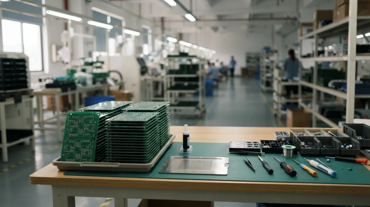
The sprint where the PCB was the bottleneck
A lot of hardware teams learn the same painful lesson: your code can be ready, your enclosure can be printed, your firmware can even be flashed… and then the PCB shows up weeks later. That delay doesn’t just push a delivery date. It multiplies work: parts get reordered, test plans get rescheduled, and every subsequent revision becomes harder because time pressure squeezes the design-review loop.
So the appeal of a seven-day PCB turnaround is obvious: ship hardware on a clock, not on a queue. But what does “seven days” really mean in technical terms? And what engineering choices make it possible—without turning quality into a guess?
First, the basic cast: PCB, BOM, and manufacturing files
Let’s ground the terminology, because the fastest schedule still depends on correct inputs.
A PCB (printed circuit board) is the rigid “wiring board” where conductive copper traces connect component pads.
A BOM (bill of materials) is a comprehensive list of every part needed to build the product, including quantities and specifications. A BOM is the blueprint for procurement and assembly planning. (autodesk.com)
In practice, a PCB fab and a PCB assembly house need manufacturing artwork. The most common handoff format is Gerber files (industry-standard production drawings for each PCB layer, like copper, solder mask, and silkscreen). Along with Gerbers, teams provide drill files, stackup notes (layer thickness/material), and assembly documentation.
That’s why speed starts earlier than people think: if the BOM is wrong or the files need interpretation, the clock doesn’t run—it waits.
Why PCB timelines usually stretch into weeks
Even when shops market “quick-turn,” there’s a difference between possible fabrication time and end-to-end schedule time.
A useful rule of thumb from industry references: quick-turn PCB fabrication can range from about 24 hours to 7 business days, while standard production runs are often 2–3 weeks. (lcsc.com) That gap is not mystical; it’s queueing + process setup + material availability.
For rigid PCBs, one industry source describes typical standard lead time around 20 business days, with quick-turn options at multiple day-count targets. (resources.altium.com)
And the broader point holds: the “real” timeline is gated by the slowest dependency—usually not the final inspection, but something upstream:
- Components being available (or at least provably available)
- Fabrication complexity (layer count, via types, materials)
- Assembly complexity (fine-pitch parts, BGA, dense mixed technology)
- Rework probability (design files that are almost right are still not right)
What seven days forces you to do differently
A seven-day turnaround requires the workflow to become more deterministic. The most common technical pattern is parallelization: instead of treating sourcing, fabrication, assembly, and testing as strictly sequential phases, the schedule overlaps them so no single step dominates wall-clock time.
1) “DFM” becomes a schedule feature
DFM (design for manufacturability) is the set of checks that ensure a PCB design can be reliably produced with the selected fab process. In beginner terms: DFM tries to prevent the moment where the factory says “we can make it… but probably not the way you intended.”
For PCB land patterns (where a component pad connects mechanically and electrically), a major industry reference is IPC-7351, which standardizes guidance for surface-mount land pattern design and geometry. (ipc.org)
When DFM goes well, yield risk drops. When yield risk drops, the factory can plan for fewer surprises—and fewer surprises are the difference between 7 days and 17.
2) The BOM has to be buildable, not just correct
A BOM can be “correct” in the engineering sense (right part numbers in a spreadsheet) but still not be buildable in the manufacturing sense (lead time, packaging, alternates, or substitutions).
BOM buildability is where domestic/controlled supply chains can matter: the schedule can only be trusted if the parts procurement plan has fewer unknowns. Even without naming a specific supplier, the technical concept is the same—if sourcing isn’t locked early, the PCB is waiting.
3) Traceability turns “quality” into evidence
A fast turnaround is scary unless you also demand fast evidence. That’s where traceability shows up.
In electronics manufacturing, traceability is the ability to follow materials, production steps, inspection data, testing results, and shipment records across the manufacturing process. (bestpcbs.com) In higher-stakes contexts, IPC even publishes a standard specifically about manufacturing and supply chain traceability of electronic products (with risk-based minimum requirements). ()
In a seven-day model, traceability isn’t bureaucracy—it’s what makes “we shipped fast” defensible.
Concretely, traceability usually includes:
- Component lot and revision linkage
- PCB serial or batch identification
- Process parameters or inspection results
- Test outcomes tied back to the specific built unit(s)
4) Standards are the guardrails against rushed workmanship
Speed increases the temptation to “accept by vibe.” Quality standards exist to remove vibes from the loop.
For assembly acceptance, IPC-A-610 is a widely used standard describing visual acceptability requirements for electronic assemblies. () For soldering process requirements and acceptance criteria, IPC J-STD-001J describes materials, methods, and acceptance criteria intended to rely on process control methodology. ()
The key for schedule thinking: when both sides agree on the acceptance basis, you reduce the chance that a late-stage disagreement forces a restart.
A realistic “seven business days” mental model
To understand what “Day 0 through Day 7” tends to mean technically, picture the workflow as dependency edges:
- You approve a quote and confirm the build (this is where the schedule clock starts).
- That approval unlocks procurement, fabrication release, and assembly programming.
- You don’t wait for one step to finish before starting the next; you align them.
A simplified timeline might look like this:
Day 0 (approval)
 - BOM/buy plan locked
 - Fabrication files released (Gerbers → fab toolpath)
 - Assembly program created (pick-and-place jobs, paste stencil data)

Day 1–2
 - PCB fabrication begins
 - Parts sourcing continues (or ships arrive)

Day 3–4
 - Fabricated panels move into assembly
 - Solder paste printing + component placement setup

Day 5
 - Reflow (the oven profile step)
 - Automated optical inspection (AOI) begins

Day 6–7
 - X-ray or other inspections (for hidden joints where relevant)
 - Functional/in-circuit testing as required
 - Packaging and shipment record generation
Notice what’s missing: there’s no “mystery research” step. Every action has to be pre-planned because the schedule window is too small for uncertainty.
Revisions without a restart: how revs stay fast
One subtle engineering idea behind fast iteration is revision continuity.
In many teams, a revision number (Rev A → Rev B → Rev C) becomes a scheduling cliff: the factory discards work done for the prior version, regenerates everything, and rechecks everything. A seven-day approach tries to treat later revisions as deltas—picking up where the last rev left off—so you’re not paying full setup cost each time.
That only works when revision control is disciplined:
- The build package is versioned (which BOM, which Gerbers, which assembly drawings?)
- The DFM results are tracked (what changed and did it invalidate manufacturability assumptions?)
- The testing artifacts are linked to the right revision
Why this is ultimately a system, not a trick
So what’s the “secret” behind getting boards in days instead of weeks?
It’s not magic solder. It’s process design under constraint.
When a factory can compress timelines, it typically means:
- Quick-turn fabrication is treated as a real capability (not a vague promise), consistent with reference timelines that range from 24 hours to 7 business days versus multi-week standard runs. (lcsc.com)
- The BOM is procurement-ready, not only design-ready. (autodesk.com)
- Traceability and acceptance standards are in place so “fast” doesn’t become “unknown.” (bestpcbs.com)
- Land pattern and manufacturability guidance are aligned with established references like IPC-7351. (ipc.org)
And that leads to a sharper question hardware engineers often end up asking: Why does a PCB order still behave like a multi-week project even when the fabrication step can be quick? The answer is dependencies—most of them upstream of the moment you see copper.
Closing thought: speed is engineering clarity
Seven-day PCB turnaround is less about sprinting at the end and more about removing uncertainty at the beginning. Once DFM checks, BOM buildability, traceability evidence, and acceptance standards line up, the schedule stops wobbling.
That’s the real win: faster hardware iteration driven by clarity, not rushed improvisation.
Comments (0)
No comments yet. Be the first to respond!
Leave a Comment
Your comment will be visible after review.